Date: 10/03/2023 13:39:16
From: SCIENCE
ID: 2005063
Subject: InfraRedInSitu
SCIENCE said:
Can’t see infra red.
What does it say?
The Rev Dodgson said:
SCIENCE said:
Can’t see infra red.
What does it say?
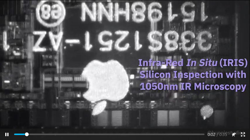
“Infra-Red, In Situ” (IRIS) inspection. It is founded on two insights: first, that silicon is transparent to infra-red light; second, that a digital camera can be modified to “see” in infra-red, thus effectively “seeing through” silicon chips. We can use these insights to inspect an increasingly popular family of chip packages known as Wafer Level Chip Scale Packages (WLCSPs) by shining infrared light through the back side of the package and detecting reflections from the lowest layers of metal using a digital camera. This technique works even after the chip has been assembled into a finished product. However, the resolution of the imaging method is limited to micron-scale features.